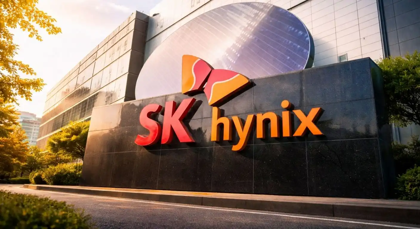
The global race for artificial intelligence supremacy just shifted into a higher gear. South Korean semiconductor leader SK Hynix announced on Wednesday that it has officially begun shipping samples of its next-generation 12-layer HBM4E memory chips to major global technology customers. This milestone underscores the company’s aggressive strategy to maintain its dominant lead in the high-bandwidth memory market, a sector that serves as the backbone for the world’s most powerful AI processors.
These new HBM4E chips represent a massive leap in technical capability. By stacking 12 individual layers of memory into a single package, SK Hynix has significantly increased both data capacity and processing speed compared to its previous HBM4 models. The semiconductor giant confirmed that these samples are designed to meet the extreme demands of next-year’s flagship AI training and inference hardware. Industry experts anticipate that this component will be essential for the next generation of AI servers, which require massive memory bandwidth to process complex language models in real-time.
The timing of this announcement is no coincidence. As tech giants like Nvidia and AMD prepare for their 2027 product roadmaps, the competition to secure the best memory architecture has reached a fever pitch. SK Hynix currently holds an estimated 50% market share in the high-bandwidth memory space, a lead it has defended by consistently beating rivals to market with higher layer counts and more efficient designs. This latest move signals that the company is not ready to slow down anytime soon.
Financial analysts expect these HBM4E products to drive significant growth for the company over the next 18 months. With the AI infrastructure market projected to reach $500 billion by 2028, high-performance memory has become the most valuable commodity in the chip world. SK Hynix has already invested over $10 billion in research and development and new manufacturing facilities in South Korea to ensure it can scale production of these complex 12-layer stacks quickly once customer testing concludes.
One of the greatest challenges in manufacturing HBM4E is the thermal management of 12-layer structures. SK Hynix engineers addressed this by utilizing a new proprietary base die technology that improves heat dissipation by approximately 15%. This improvement is crucial, as modern AI data centers struggle with intense heat loads that can degrade hardware performance over time. By solving this bottleneck, the company is making its memory modules more attractive to data center operators who want to lower their electricity costs while increasing computing output.
While SK Hynix leads the pack, its competitors—including Samsung and Micron—are working around the clock to close the gap. However, the complexity of manufacturing these advanced memory stacks acts as a high barrier to entry. Industry insiders suggest that mass production of these 12-layer HBM4E units will likely begin in early 2027, just in time for the anticipated launch of next-generation AI enterprise hardware.
As the tech world watches this development, the broader impact on the global supply chain remains clear. The demand for HBM memory is currently outpacing supply by nearly 20%, creating a seller’s market that continues to boost SK Hynix’s bottom line. For the end user, this race means that AI tools will become faster, more accurate, and more capable of handling massive datasets without crashing. SK Hynix is betting that its early delivery of these high-performance samples will make it the default choice for the AI hardware of tomorrow.